Cadence Projects in Bangalore
Cadence Analog & Digital IC Design Projects 2026 — IEEE Projects for BE, MTech & PhD Engineers in BangaloreCadence Design Systems provides the industry's most widely used EDA (Electronic Design Automation) suite for custom analog, mixed-signal and digital integrated circuit design — used by every major semiconductor company from Qualcomm to Intel. At ProjectsatBangalore, we deliver 18+ IEEE 2025–2026 Cadence projects for BE, MTech and PhD students across two major design domains: Analog & Mixed-Signal IC Design — covering low-power operational amplifiers, CMOS analog filters and voltage-controlled oscillators (VCOs) — and Digital IC Design — covering high-speed multipliers, logic synthesis and place & route. Every project uses the complete Cadence toolchain: Cadence Virtuoso for schematic capture and custom layout, Cadence Spectre for SPICE-accurate circuit simulation, Cadence Genus for RTL logic synthesis, Cadence Innovus for digital place and route, Cadence Tempus for signoff static timing analysis (STA), and Cadence Voltus for power integrity and IR-drop analysis. Each project follows the full workflow — schematic design, layout design generation, and DRC/LVS verification — and includes IEEE Xplore base paper reference, complete Cadence design files, simulation waveforms, university-format report for VTU/Anna University/JNTU, PPT and viva Q&A support.
Cadence Project Domains We Cover
- Low-power operational amplifier design (two-stage, folded-cascode)
- CMOS analog filter design (Gm-C, switched-capacitor, active-RC)
- Voltage-controlled oscillator (VCO) design — ring and LC-tank
- High-speed multiplier design (Wallace tree, Booth, array)
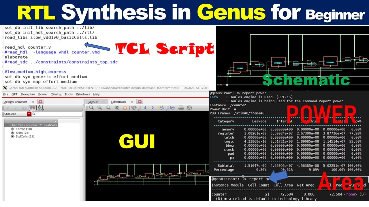
- Digital logic synthesis using Cadence Genus
- Place and route using Cadence Innovus
- Static timing analysis using Cadence Tempus (signoff STA)
- Power integrity and IR-drop analysis using Cadence Voltus
- Mixed-signal IC design (ADC, DAC, bandgap reference, comparator)
- RF building blocks (LNA, mixer, PLL) using Cadence Spectre RF
- Analog and mixed-signal layout design in Cadence Virtuoso
- DRC/LVS physical verification and parasitic extraction (PEX)
CADENCE Based Projects
Cadence EDA Tools & Design PlatformsAll Cadence Design Systems tools used across our 18+ IEEE 2026 analog, mixed-signal and digital IC design Cadence projects for BE, MTech and PhD students in Bangalore.
Cadence Related Projects
Analog & Mixed-Signal IC Design — Key Building BlocksAll key analog and mixed-signal circuit blocks designed in Cadence Virtuoso and simulated with Cadence Spectre across our IC design Cadence projects.
| # | IEEE 2026 Cadence Project Topic | Cadence Tool | Technology |
|---|---|---|---|
| 01 | Design and Layout of a Two-Stage Miller-Compensated Low-Power Operational Amplifier IEEE 2026 | Virtuoso, Spectre, ADE | GPDK 180nm/90nm |
| 02 | Low-Power Folded-Cascode Operational Amplifier with Enhanced Slew Rate for Biomedical Applications IEEE 2026 | Virtuoso, Spectre | GPDK 90nm |
| 03 | Rail-to-Rail Low-Power Operational Amplifier Design for Sub-1V Supply Analog IC Applications IEEE 2025 | Virtuoso, Spectre, ADE | GPDK 45nm |
| 04 | Subthreshold Operation Ultra-Low-Power Op-Amp for Wearable IoT Sensor Front-End Design IEEE 2026 | Virtuoso, Spectre | GPDK 65nm |
| # | IEEE 2026 Cadence Project Topic | Cadence Tool | Technology |
|---|---|---|---|
| 05 | Design of a Fifth-Order Gm-C Low-Pass CMOS Analog Filter for Biomedical Signal Conditioning IEEE 2026 | Virtuoso, Spectre, ADE | GPDK 180nm |
| 06 | Tunable Switched-Capacitor CMOS Analog Filter for Software-Defined Radio Channel Selection IEEE 2026 | Virtuoso, Spectre | GPDK 90nm |
| 07 | Active-RC Butterworth CMOS Analog Filter Design with Automatic Frequency Tuning Loop IEEE 2025 | Virtuoso, Spectre, ADE | GPDK 65nm |
| # | IEEE 2026 Cadence Project Topic | Cadence Tool | Technology |
|---|---|---|---|
| 08 | Design and Phase Noise Analysis of a Three-Stage CMOS Ring Voltage-Controlled Oscillator IEEE 2026 | Virtuoso, Spectre, ADE | GPDK 180nm |
| 09 | Low Phase-Noise LC-Tank VCO Design for 5G NR RF Frequency Synthesizer Front-End IEEE 2026 | Virtuoso, Spectre RF | GPDK 65nm |
| 10 | Wide Tuning Range Current-Starved Ring VCO Design for PLL Clock Generation Applications IEEE 2025 | Virtuoso, Spectre, ADE | GPDK 90nm |
| # | IEEE 2026 Cadence Project Topic | Cadence Tool | Technology |
|---|---|---|---|
| 11 | RTL-to-GDSII Implementation of an 8x8 Wallace Tree High-Speed Multiplier Using Cadence Genus and Innovus IEEE 2026 | Verilog, Genus, Innovus, Tempus | GPDK 90nm |
| 12 | Low-Power 16x16 Booth Multiplier Synthesis and Place-and-Route Using Cadence Genus and Innovus IEEE 2026 | Verilog, Genus, Innovus, Voltus | GPDK 65nm |
| 13 | High-Speed Carry-Save Adder Based Array Multiplier with Static Timing Signoff Using Cadence Tempus IEEE 2025 | Verilog, Genus, Innovus, Tempus | GPDK 45nm |
| 14 | Power and Area Optimised Vedic Multiplier Design with Logic Synthesis Using Cadence Genus IEEE 2025 | Verilog, Genus, Innovus | GPDK 90nm |
| # | IEEE 2026 Cadence Project Topic | Cadence Tool | Technology |
|---|---|---|---|
| 15 | Full RTL-to-GDSII Flow of an 8-Bit RISC ALU Datapath Using Cadence Genus, Innovus, Tempus and Voltus IEEE 2026 | Genus, Innovus, Tempus, Voltus | GPDK 45nm |
| 16 | Clock Tree Synthesis and IR-Drop Analysis of a Pipelined Processor Datapath Using Innovus and Voltus IEEE 2026 | Innovus, Voltus, Tempus | GPDK 65nm |
| 17 | Multi-Corner Multi-Mode (MCMM) Static Timing Analysis Signoff Using Cadence Tempus for a UART Core IEEE 2025 | Genus, Innovus, Tempus | GPDK 90nm |
| 18 | Floorplanning, Power Planning and Detailed Routing of a FIFO Memory Controller Using Cadence Innovus IEEE 2025 | Genus, Innovus, Voltus | GPDK 45nm |
| # | IEEE 2026 Cadence Project Topic | Cadence Tool | Technology |
|---|---|---|---|
| 19 | Design of a Curvature-Compensated CMOS Bandgap Voltage Reference for Mixed-Signal IC Applications IEEE 2026 | Virtuoso, Spectre, ADE | GPDK 180nm |
| 20 | 8-Bit Successive Approximation Register (SAR) ADC Design with Sample-and-Hold Front-End IEEE 2026 | Virtuoso, Spectre, ADE | GPDK 90nm |
| 21 | High-Speed Dynamic Latch Comparator with Hysteresis Design for Mixed-Signal Pipeline ADC IEEE 2025 | Virtuoso, Spectre | GPDK 65nm |
| # | IEEE 2026 Cadence Project Topic | Cadence Tool | Technology |
|---|---|---|---|
| 22 | Design of a 2.4 GHz Low-Noise Amplifier (LNA) for 5G/WiFi RF Front-End Using Cadence Spectre RF IEEE 2026 | Virtuoso, Spectre RF | GPDK 65nm |
| 23 | Double-Balanced Gilbert-Cell RF Mixer Design with Conversion Gain Optimisation Using Cadence Spectre IEEE 2025 | Virtuoso, Spectre RF | GPDK 90nm |
Cadence Projects VLSI
Cadence Workflow Steps for Analog & Layout ProjectsThe standard 6-step Cadence design flow followed in every analog and mixed-signal IC design project — from schematic design to layout design generation and complete physical verification.
Schematic Design (Schematic Capture)
The circuit topology is captured in Cadence Virtuoso Schematic Editor using GPDK 45nm/65nm/90nm/180nm technology library devices — sizing transistor widths and lengths, setting bias currents, and adding ports/pins for the design under test.
Cadence Virtuoso Schematic EditorSimulation Setup in ADE (Analog Design Environment)
DC operating point, AC frequency response, transient, noise and Monte-Carlo process-variation analyses are configured in ADE-L/ADE-XL and run using the Cadence Spectre SPICE-accurate simulator to verify gain, bandwidth, phase margin, slew rate and power.
Cadence Spectre + ADE-L / ADE-XLLayout Design Generation
The physical layout is drawn in Cadence Virtuoso Layout Suite, applying analog layout best practices — common-centroid matching for differential pairs, dummy devices, guard rings for noise isolation, and symmetric routing for sensitive analog nodes.
Cadence Virtuoso Layout SuitePhysical Verification — DRC & LVS
Design Rule Check (DRC) confirms the layout obeys all foundry geometric rules (spacing, width, enclosure), while Layout Versus Schematic (LVS) confirms the extracted layout netlist exactly matches the original schematic — both run using Calibre or Cadence Pegasus.
Calibre / Cadence Pegasus DRC+LVSParasitic Extraction (PEX)
Once DRC/LVS is clean, parasitic resistance and capacitance are extracted from the physical layout to generate a post-layout (extracted) netlist that accurately represents real silicon interconnect effects.
Cadence Quantus / StarRCPost-Layout Simulation & Signoff
The extracted netlist is re-simulated in Cadence Spectre to validate real performance with parasitics included — final gain, bandwidth, phase margin, power and noise results are compared against pre-layout targets before tapeout-ready signoff.
Cadence Spectre Post-Layout SimCadence Project Ideas
Frequently Asked Questions — Cadence ProjectsCommon questions students ask about Cadence Virtuoso, Spectre, Genus, Innovus, Tempus and Voltus projects for BE, MTech and PhD.
Cadence Virtuoso for Students
Cadence Virtuoso Projects - Lab Gallery — BangaloreA look inside our Cadence analog, mixed-signal and digital IC design lab — Virtuoso, Spectre, Genus, Innovus, Tempus and Voltus project setups for BE, MTech and PhD scholars in Bangalore.
 Cadence Virtuoso Analog Lab
 Cadence Spectre Simulation
 Genus / Innovus Digital Flow
 Tempus / Voltus STA & Power